
As a maker, I all the time wanted to create a PCB (printed circuit board) on-line but making PCBs always appeared like a tedious activity. Then I got here across a free on-line software called EasyEDA. In this article, I will show you how you can get began with EasyEDA to start creating skilled PCBs on your initiatives. For this venture, I’ll stroll you through the means of designing and manufacturing a PCB for an IR Proximity Sensor. First, we have to plan the design by drawing a circuit diagram on paper. Once the diagram is complete, we can make a prototype on a breadboard to check out the circuit. Make adjustments to the circuit drawing as needed.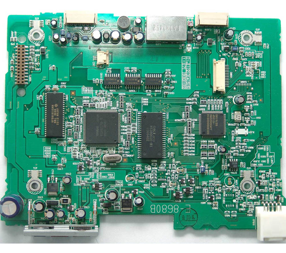 Now that we’ve a working circuit, we are able to finalize the design in software. There are various online tools to make custom PCBs online. For this mission, we will use EasyEDA. If you have any concerns pertaining to the place and how to use pcba (Highly recommended Reading), you can get in touch with us at our own internet site. Here you can either download the software or use the net designer. Then, click on the EasyEDA Designer to make use of the web instrument. Now, PCB board we have to create an account with EasyEDA. Click on “Projects” and “Log in” from the left menu. Create an account or sign up. Next click on on “New Project.” Give the project a name and outline. I named the challenge “IR Proximity Sensor. Save the undertaking. You’ll discover a blank canvas. Some part symbols on the left facet. You’ll notice a clean canvas. Some half symbols on the left facet. We are going to use these components to make our design. If you can’t discover an element, you can look within the Libraries. Just search for the half you’re searching for. Be certain that it has a logo. Double-click on on the part to pick it, and place it on the canvas. Then seek for the next part. Repeat this process for the remaining components. Use your hand-drawn circuit diagram to create a digital circuit. Draw the wires by clicking on the tip of one half. The terminal of the opposite part. 5V represents the ability connections. If you find yourself pleased with the design, convert this circuit into a PCB. To do this, first, click on on the PCB option from the highest menu (next to the star icon). EasyEDA might ask you to check the nets or connections, however you may skip this in case you are certain your connections are correct. You will see a new tab with a border. Components which you must arrange on the board. Start arranging the elements on the board. Ensure you place these components physically closer that are linked instantly. This will make routing easier and less complicated. After inserting all the parts we will start routing. PCB Routing is whenever you add traces that may connect parts. As a hobbyist, we are going to make 2-layer PCBs because they are extra affordable to manufacture. The pink traces symbolize the highest layer. The blue traces signify the underside layer. You may all the time add more layers, however they are going to increase the price of your board. EasyEDA also has an Autorouter tool which can make the traces for you. This device works nice for small. Less complex circuits however it’d make errors in big initiatives. I recommend manual routing. Listed below are some key issues to think about when wiring traces in your PCB design. 1. Use thicker tracks for power strains. 2. Avoid 90° turns whereas making traces. Traces would possibly get etched off easily at 90°. Also, it tends to trigger a whole lot of noise in the circuit which may affect Wireless purposes. 3. Don’t connect GND traces. Use the copper space instrument at the top to create a single ground plate. 4. Make certain you keep a very good clearance between traces. Ground plates to avoid any short circuits. Make sure that you retain a superb clearance between traces. Ground plates to avoid any quick circuits. 5. Never make traces close to the sting of the PCB or the screw holes. Once you are glad along with your traces, double-verify the routes, and save the PCB file. You’ll be able to see how the product will look after manufacturing before producing the PCB information (also referred to as Gerber files). Open the 3D viewer in EasyEDA by clicking on the digital camera icon in the highest bar and selecting “3D viewer”. The 3D mannequin will take a few seconds to load. Use this model to see how the final board will look. Once you’re glad with the look, return to the PCB tab and click on the G icon. You will discover a window to verify the routes. If you click on on “yes,” the software program will show you routing errors. Be aware that if you happen to used flags or ports to name a pin and later made the connections, it can present these connections as an error. Once you might be positive the connections are right, transfer to the subsequent step. You will notice a pop-up window like under. Here you possibly can obtain the Gerber recordsdata and send them to any PCB producer (Get $5 Free on PCBWay) or order them directly from OshPark or JLCPCB. It is a primary tutorial to get you began with PCB designing. Now you can begin converting your breadboard prototypes into professional-looking PCBs.